Last updated: January 24, 2003
|
1. Change Gain Structure
Changed the gain structure so that it makes more sense to me. I wanted each of the three attenuators to be able to provide a slight bit of amplification without having to rely on the mixer section to provide extra gain. I also wanted channels 1 and 2 to provide the same output level regardless of whether the outputs were being tapped from OP1/OP2 or from +OP.
Procedure
- Change R3, R5, R14 from 22K to 24K so that each of the three reversing attenuators will provide slightly more than unity gain.
- Change R20 from 51K to 47K so that the mixer section has unity gain.
- Leave out R21; unnecessary component when using Stooge panel (shown at left).
|
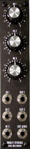
2. Normalize Inputs and Outputs
Larry Hendry has a great normalizing scheme for previous issues of the Multimix. In a nutshell, this normalizing scheme enables the Multimix to act as a 1 in 3 out distributor, a 3 in 1 out mixer, or various combinations of distributors and mixers. I adapted this scheme to the Issue 3 Multimix PCB. Using the following convention for a Switchcraft 112A jack when viewed from the back with the bevelled lug in the upper right corner: the bevelled lug in the upper right corner is GND, the lug on the left edge is the SIGNAL, and the lug on the top edge is the SWITCH.
Procedure
- Connect IN1 on the PCB to SIGNAL on the IN1 jack.
- Connect IN2 on the PCB to SIGNAL on the IN2 jack.
- Connect IN3 on the PCB to SIGNAL on the IN3 jack.
- Connect SIGNAL on the IN1 jack to SWITCH on the IN2 jack.
- Connect SIGNAL on the IN2 jack to SWITCH on the IN3 jack.
- Connect OP1 on the PCB to SIGNAL on the OUT1 jack.
- Connect OP2 on the PCB to SIGNAL on the OUT2 jack.
- Connect +OP on the PCB to SIGNAL on the OUT3/MIX jack.
- Connect IP1 on the PCB to SWITCH on the OUT1 jack.
- Connect IP2 on the PCB to SWITCH on the OUT2 jack.
- Connect a jumper between OP3 and IP3 on the PCB.
IN4 and -OP on the PCB are not used.
Larry Hendry's original Multimix normalizing scheme.
|
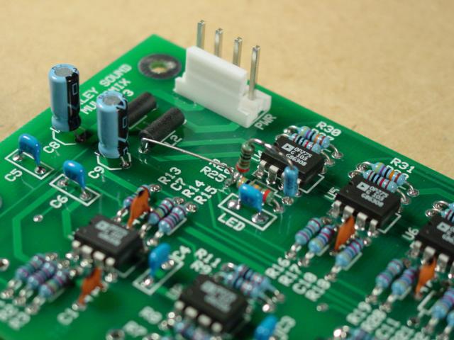
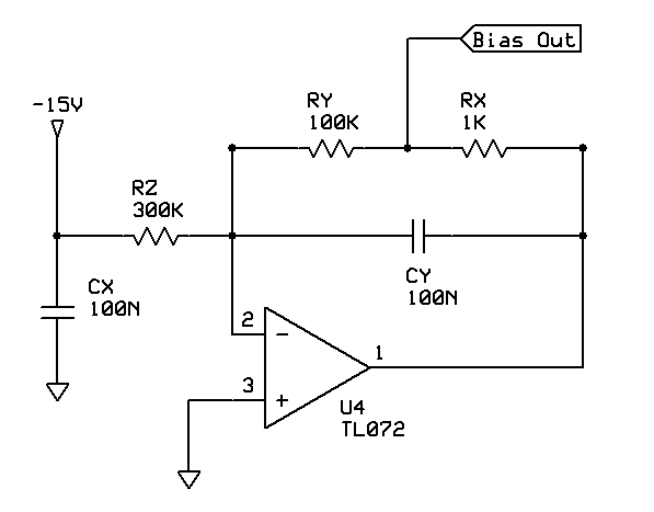
3. Add +5V Bias Circuit
Added a +5 volt bias source using the (unused) LED driver circuit built around R25, R26, and U4 (pins 1, 2, 3). By normalizing this bias source to the three attenuators, the Multimix provides up to three bias sources adjustable from -5.45 volts to +5.45 volts when nothing is plugged into the corresponding input jacks. Combined with the normalizing scheme from mod #2 above, the bias source can be applied to any of the three Multimix channels to add a DC offset to any signal. This is handy for converting a bipolar signal (+/- 5 volts) into a unipolar signal (0 to +5 volts).
Procedure
- Must break a trace going from +OP to R25. I broke a trace on the topside of the PCB where R25 connects to R16.
- Add a 300K resistor (RZ) into location where R25 is supposed to go.
- Add 100K (RY) and 1K (RX) resistors in series into location where R26 is supposed to go. RX and RY will have to stand up vertically. Use a blob of solder to connect them together. This junction is the output from the BIAS source.
- Run a jumper from -15V to the left side of RZ (the left side of RZ being nearest to L2). The nearest source of -15V is on the left side of L2 (the left side of L2 being nearest to C9).
- Add a 100N capacitor (CX) from GND to the left side of RZ (the left side of RZ being nearest to L2). I added CX to the underside of the PCB taking GND from pin 3 of U4.
- Add a 100N capacitor (CY) into location where the LED is supposed to go.
- Connect a wire from the junction of RX and RY to the switching lug of the IN1 jack on the front panel (the lug on the top edge). This will normalize the bias source to all three inputs when nothing is plugged into the input jacks (assuming that the normalizing scheme from mod #2 above has also been applied).
 |
 |
| PCB Top View |
PCB Bottom View |
|
|