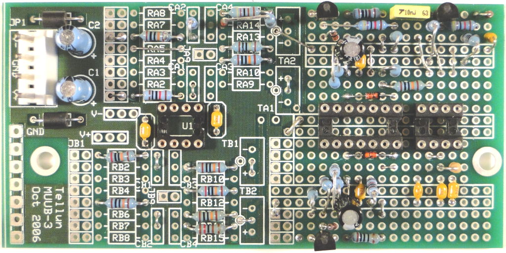
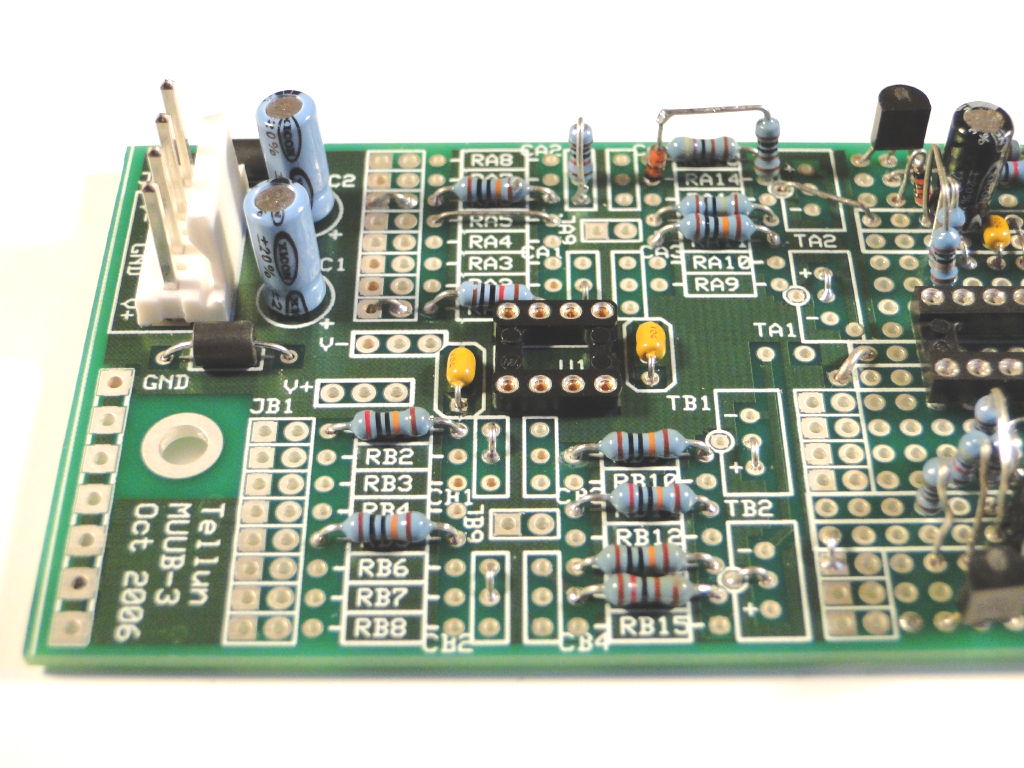
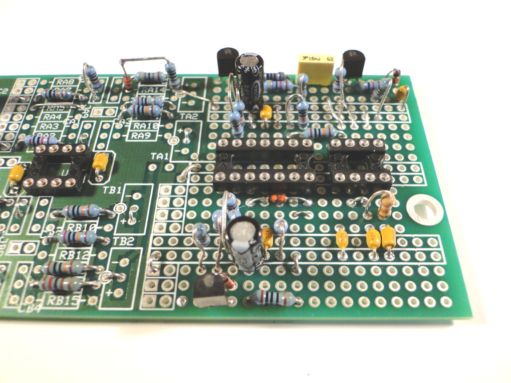
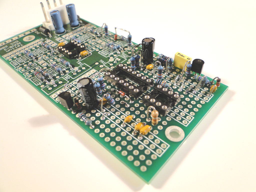
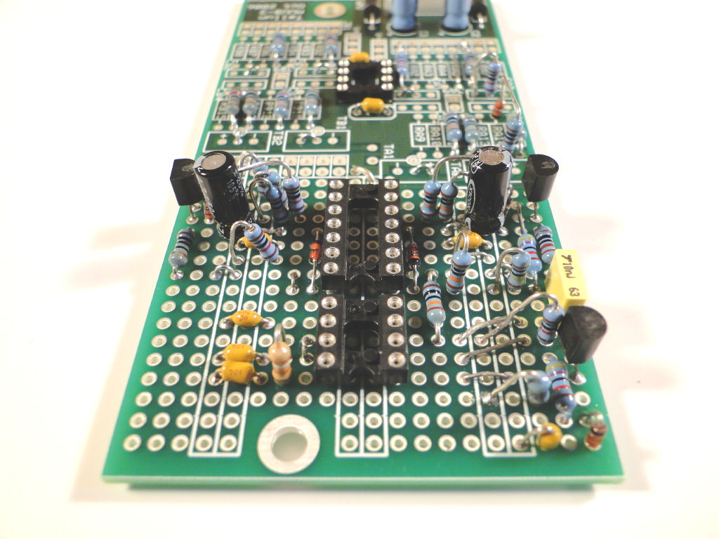
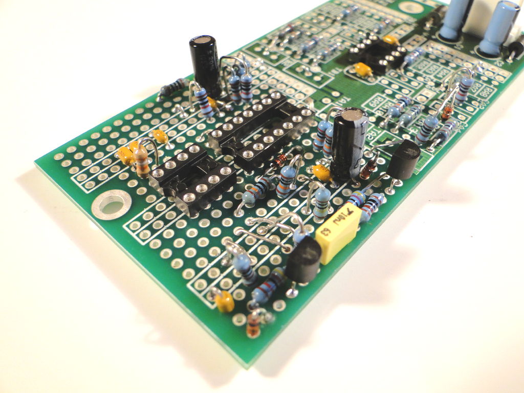
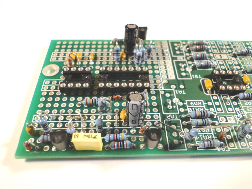
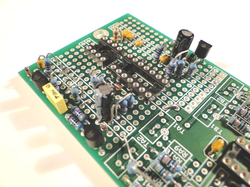
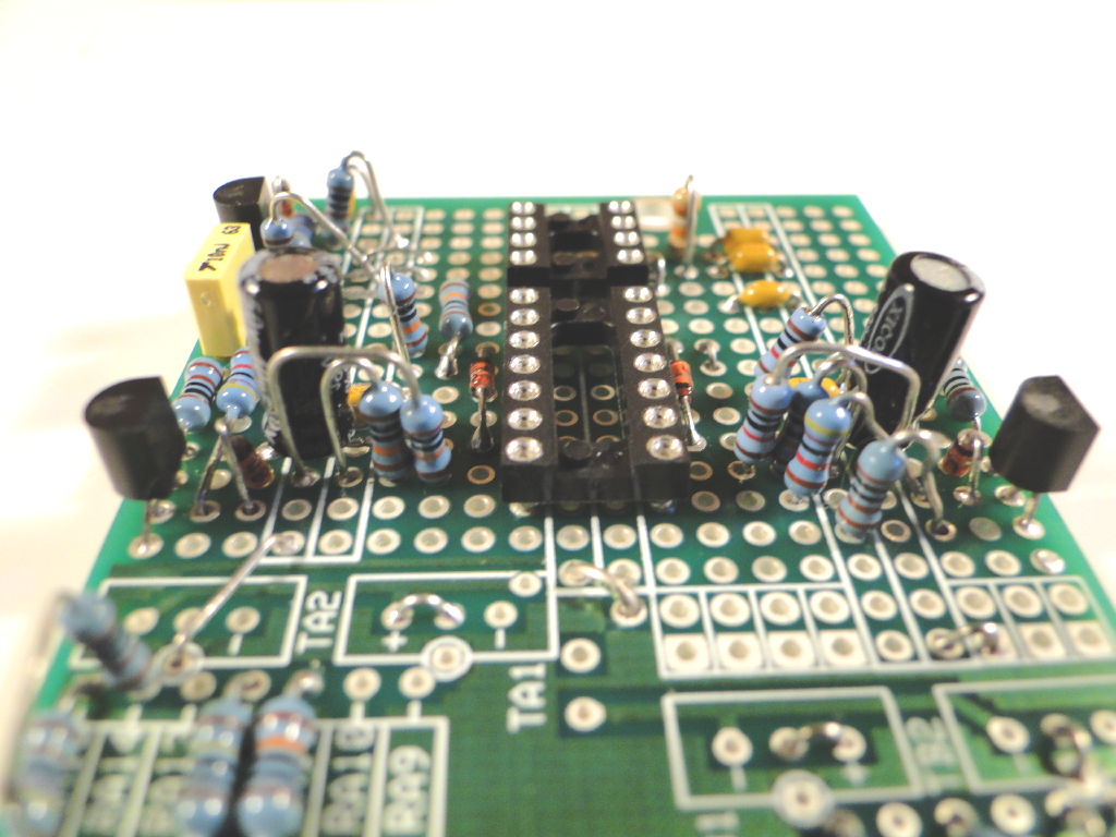
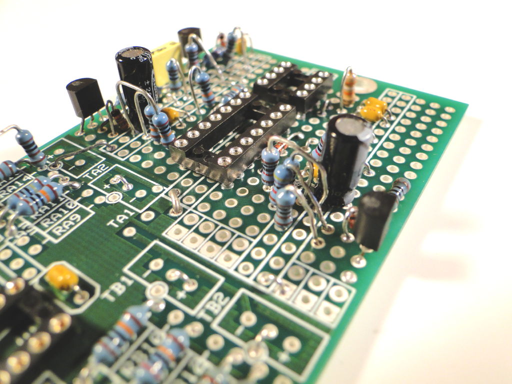
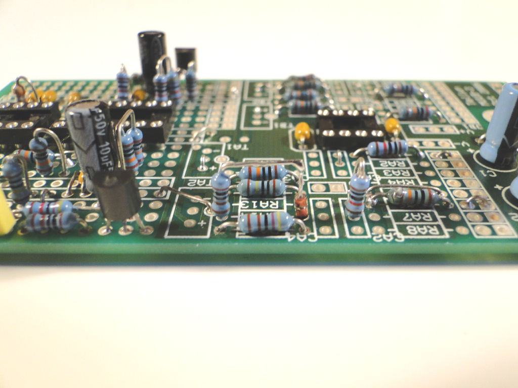
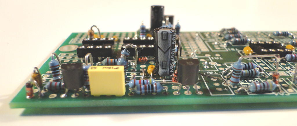
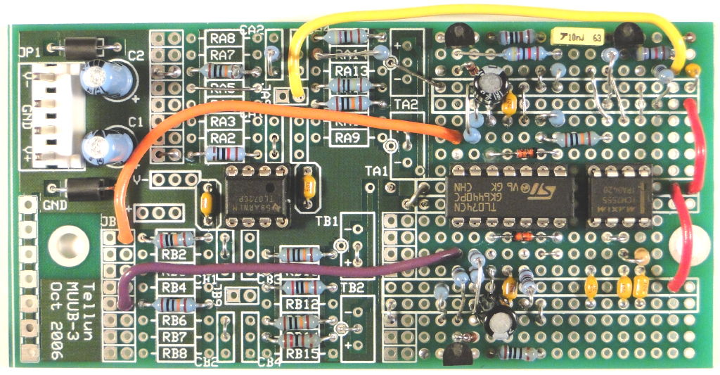
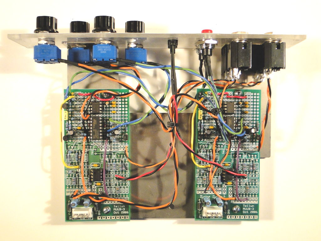
Everything from the schematic can be built onto one MUUB-3 PCB. To build a dual unit (as I did) you'll need two MUUB-3 PCBs: one for the A channel and another for the B channel. The A and B channels are constructed identically.
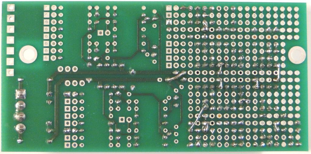
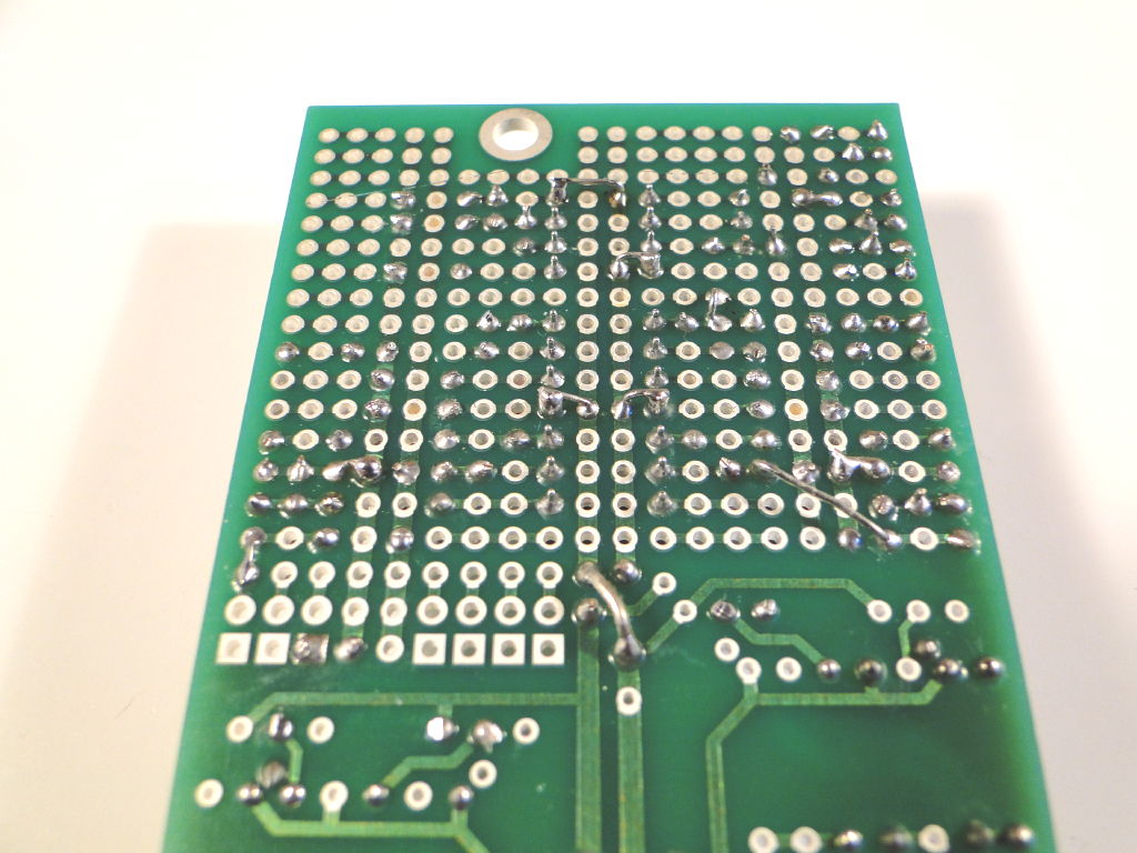
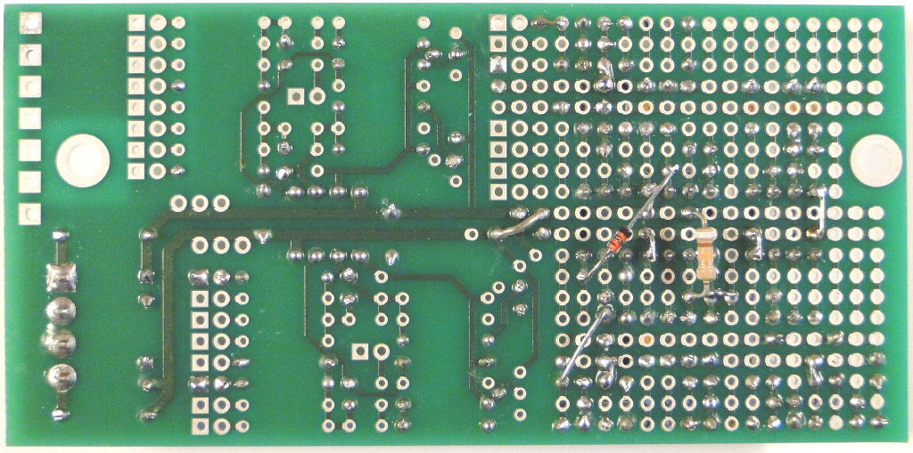
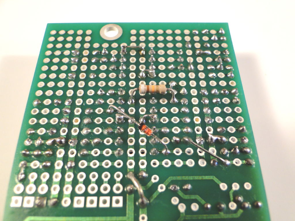
The TL072 dual op-amp on the left side of the PCB is for the input buffer and the LED driver (U1a and U1b in the schematic). Everything else is contained on the right half of the PCB in the GPA (general purpose area) using a TL074 quad op-amp and a 7555 timer. There are two busses running underneath the TL074 and 7555, one buss is for +15V, the other is for -15V. Two of the remaining four busses in the GPA are connected to ground, the other two are connected to +15V. You'll have to run jumpers from the left half of the PCB to the busses in the GPA for +15V, -15V, and ground. Most of the components can be placed on the topside of the board, but I put 1 diode, 1 resistor, and several jumpers on the underside.
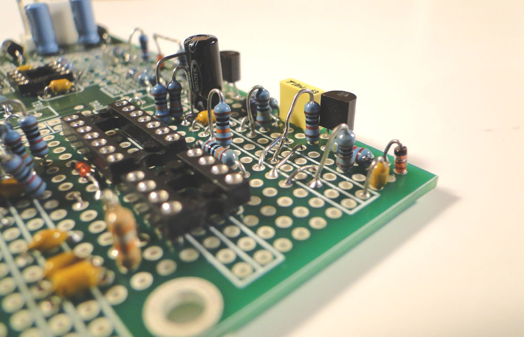
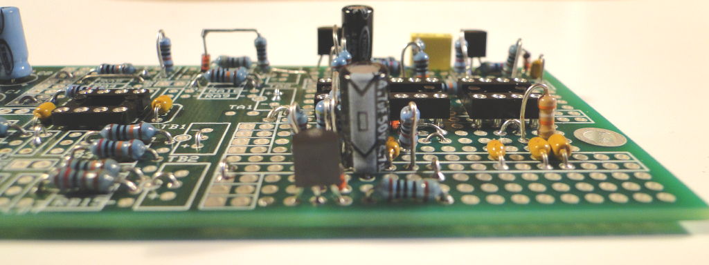
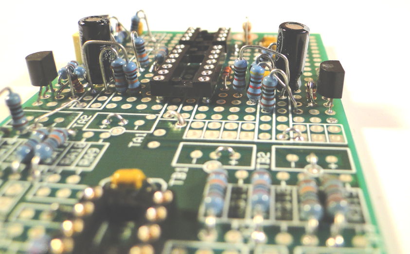
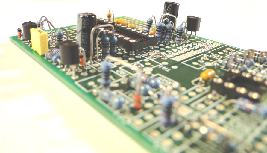
Study the pictures below to see how I put it all together.
B Channel Topside Views. The A Channel is identical:
| |
|
|
|
| |
|
|
|
| |
|
|
|
| |
|
|
|
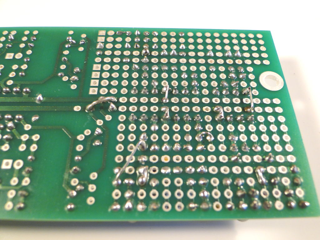
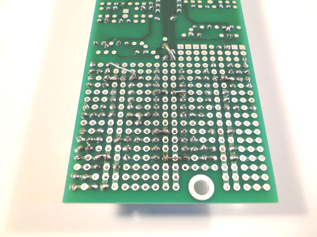
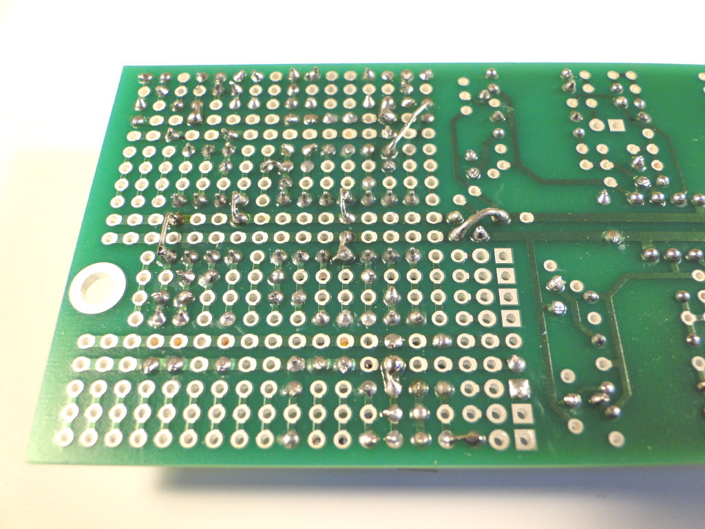
B Channel Underside Views. The A Channel is identical:
 |
 |
 |
 |
 |
 |
 |
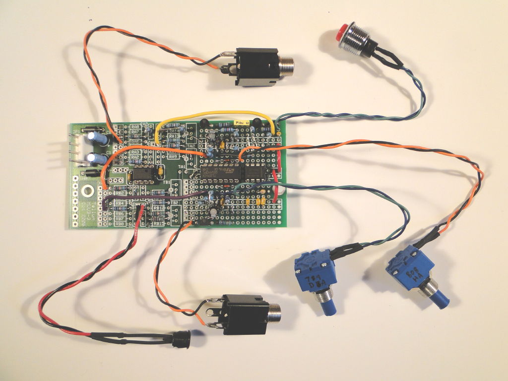
Topside Jumpers Added, Panel Components Connected, All Finished:
 |
 |
 |