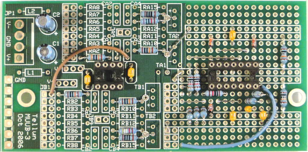
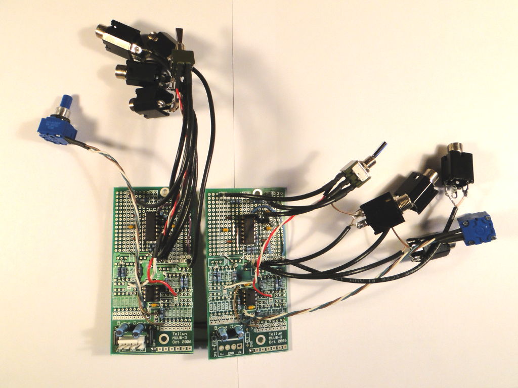
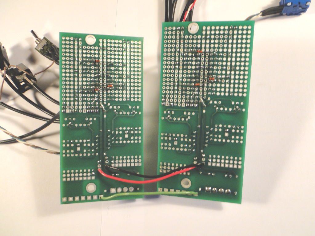
Everything from the schematic can be built onto one MUUB-3 PCB. To build a dual unit (as I did) you'll need two MUUB-3 PCBs: one for the A channel and another for the B channel. The A and B channels are constructed identically except that I only used ferrite beads and the MTA-156 power connector on one of the PCBs. I then ran power to the other PCB by running three wires from the power supply busses (+15V, -15V, and ground) between the two PCBs. Be sure to make these power supply connections after the ferrite beads.
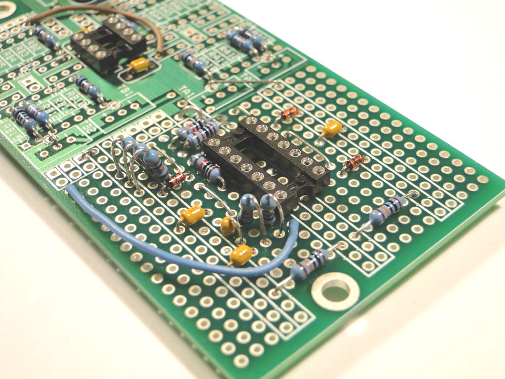
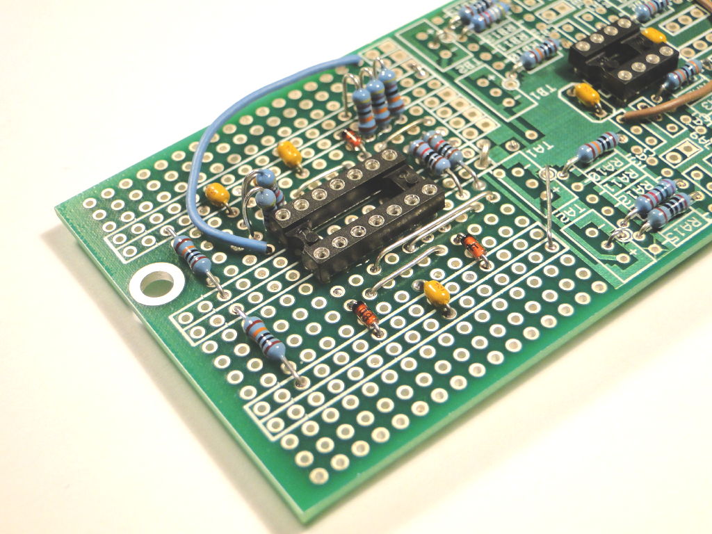
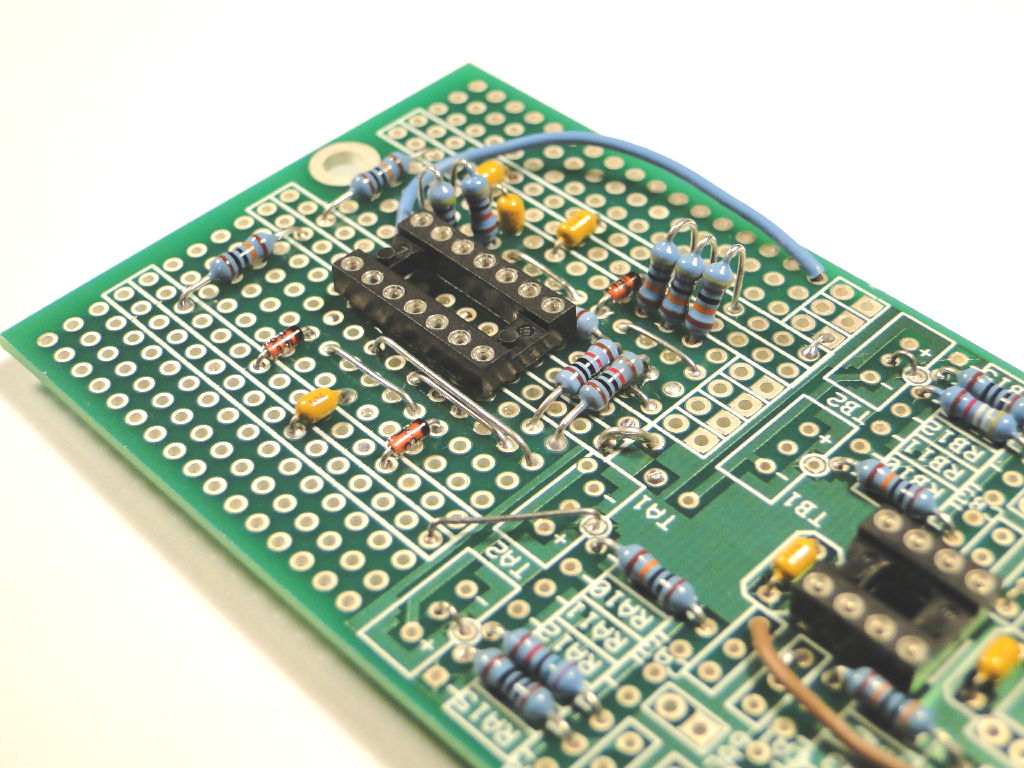
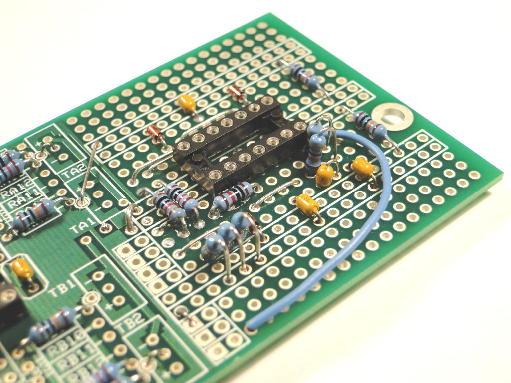
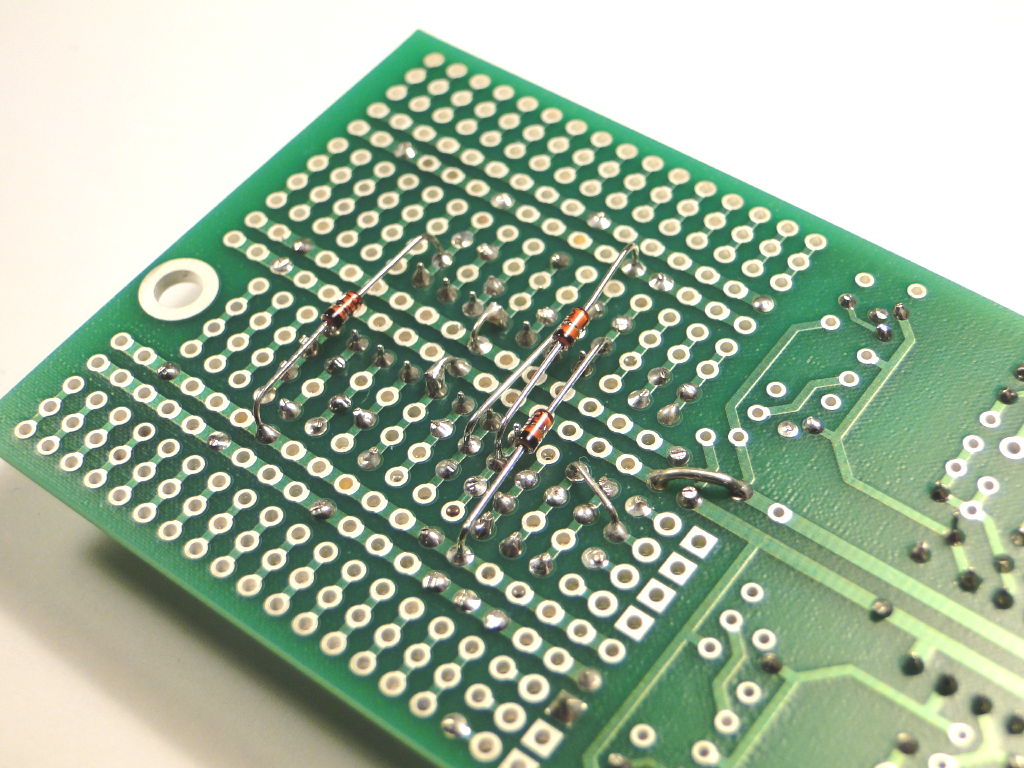
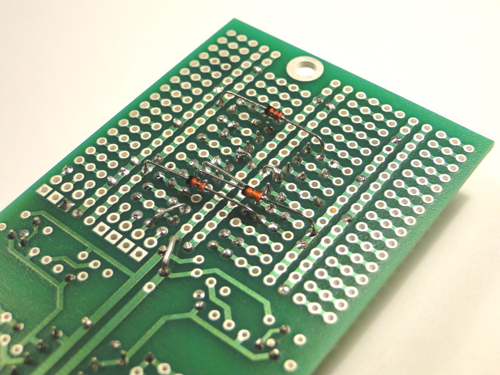
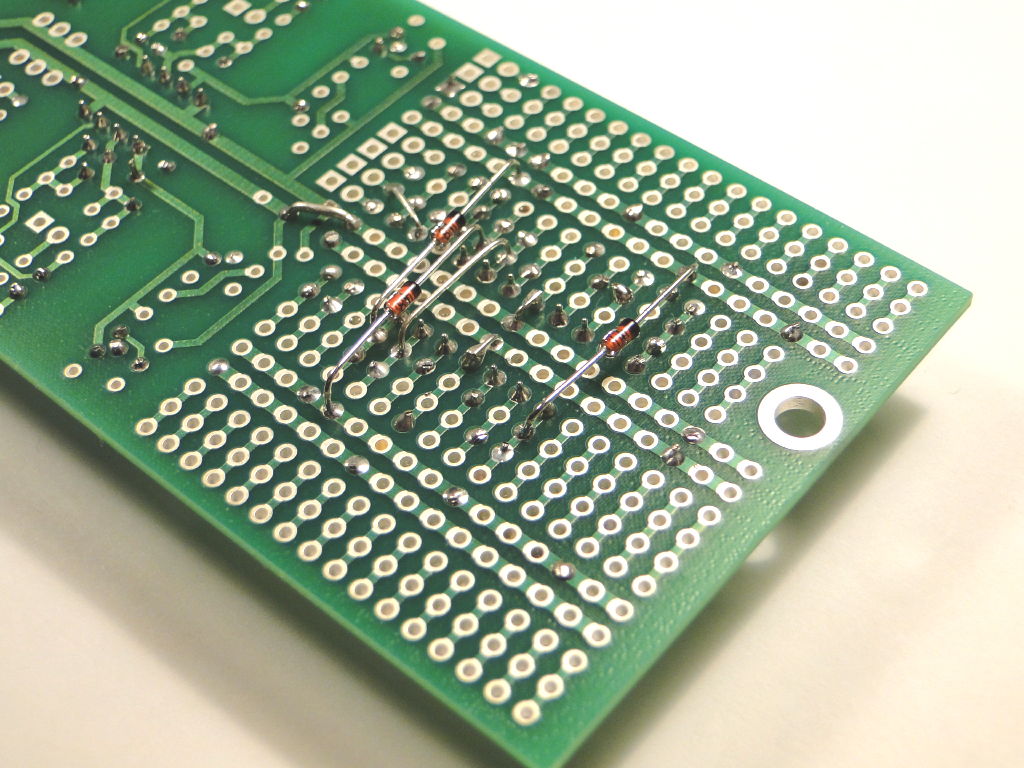
The LT1013 dual op-amp for the THRESH- and THRESH+ signals is on the left side of the PCB. Everything else is contained on the right half of the PCB in the GPA (general purpose area) using a single TL074 quad op-amp. There are two busses running underneath the TL074, one buss is for +15V, the other is for -15V. Two of the remaining four busses in the GPA are connected to ground, another buss is for the POS signal and the last buss is for the NEG signal. You'll have to run jumpers from the left half of the PCB to the busses in the GPA for +15V, -15V, and ground. Most of the components can be placed on the topside of the board, but I put 3 diodes and 2 jumpers on the underside.
Coax wires running to the front panel are best attached to the seven pads near TB1 and TB2. Three of the pads nearest the centre of the board are connected to the three IN jacks. The pad nearest the edge of the board is connected to the OUT jack.
Study the pictures below to see how I put it all together.
A Channel Topside Views. The B Channel is identical except that is has the power connector and ferrite beads:
| |
|
|
| |
|
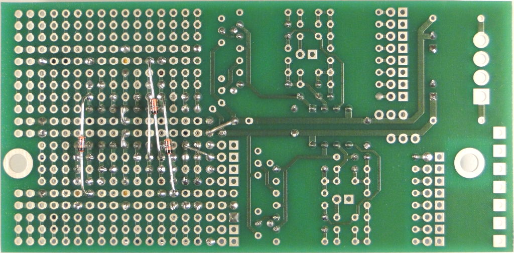
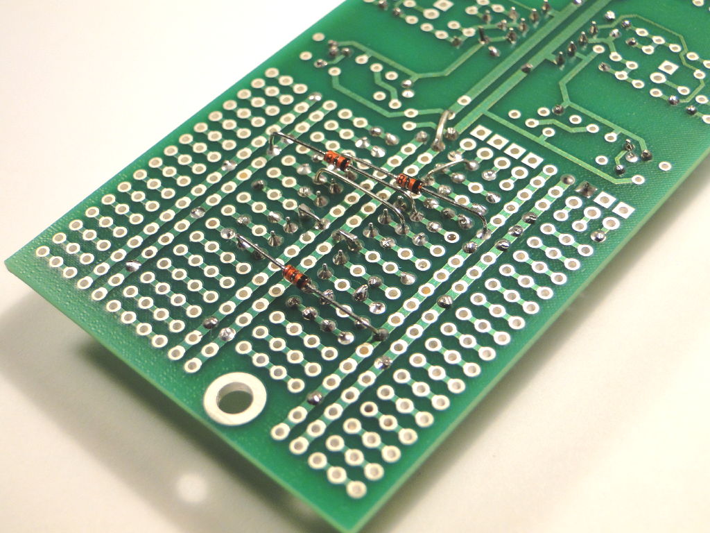
A Channel Underside Views. The B Channel is identical except that is has the power connector and ferrite beads:
 |
 |
 |
 |
 |
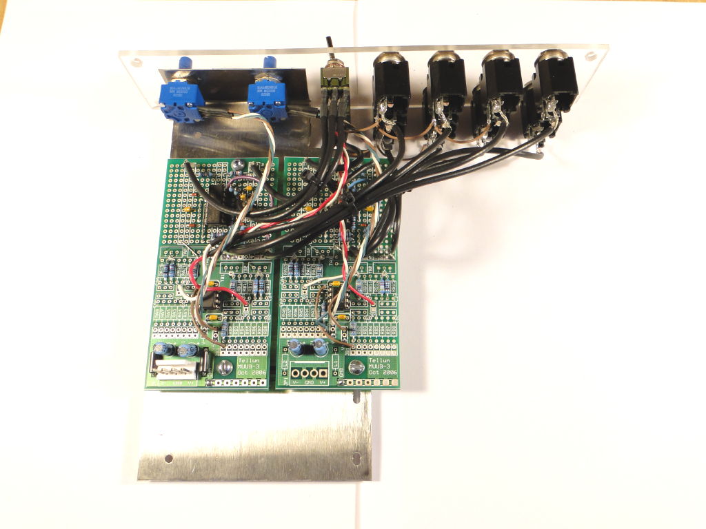
The two PCBs connected together, power supply connections between PCBs are on the underside:
 |
 |
 |